Samsung Shipping First GAAFET Silicon; 3nm and 4nm Yields Are Improving - Report
by Anton Shilov on July 18, 2023 8:30 AM EST
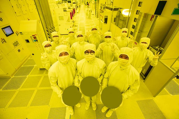
Currently, only two foundries offer their customers 3 nm and 4 nm-class process technologies: TSMC and Samsung Foundry. But business media sometimes blames Samsung Foundry for mediocre yields on leading-edge nodes, which cannot be verified. But a set of recent reports claim that Samsung is now at a point where they are shipping their first GAAFET-based 3 nm chips to commercial customers, and that the yields of Samsung's 3 nm and 4 nm-class nodes are in decent shape overall.
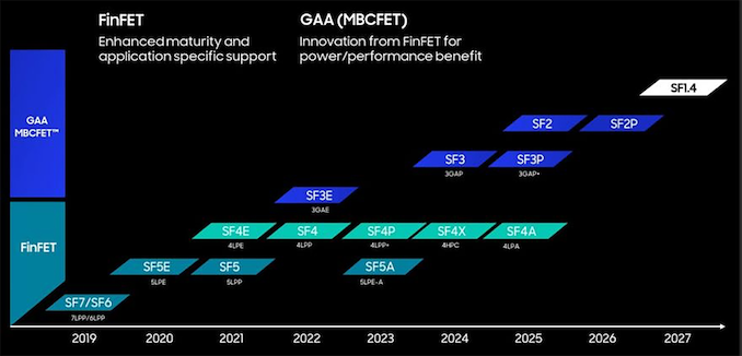
Samsung Foundry's 4 nm-class process technology yield is now higher than 75%. In contrast, yields of chips on SF3E (3nm-class, gate-all-around early) now exceeds 60%, according to estimates in a report from Hi Investment & Securities, a member of DGB Financial Group, reports Kmib.co.kr. The same report claims that TSMC's yields at its N4 node approach 80%, but again, this is an estimate by a researcher.
In general, information about yields at foundries cannot be verified since contract fabs almost never publicly talk about yields. They sometimes disclose defect density publicly compared to previous nodes, but this is hardly the case for Samsung Foundry's SF4E, SF4, SF4P, and SF3E.
Officially, Samsung Foundry only says that its SF3E process technology is in high-volume production with stable yields (possibly to address a media report from late last year which said that SF's yields on SF3E were unstable), and the development of refined SF3 is ongoing.
"We are mass producing the 1st gen 3nm process with stable yields, and, based on this experience, we are developing the 2nd gen process to secure even greater mass production capabilities," a statement by Samsung reads.
Meanwhile, TechInsights found one of the first chips made on Samsung's SF3E process. This is the Whatsminer M56S++ which is apparently a cryptocurrency mining chip from MicroBT, a Chinese developer. Mining chips are relatively simplistic devices with loads of regular structures and few SRAM bit cells. Such chips are easy to build and make for great pipe cleaners for the latest process technologies, so it is not surprising that Samsung Foundry is making them rather than large ASICs on its SF3E. Though as a reminder, smaller chips have intrinsically higher yield rates than large ASICs (lower odds of any given chip covering a flawed spot on a wafer), so the commercial viability of the Whatsminer M56S++ does not mean that a relatively large smartphone or PC SoC would hit the same yields or be equally as viable at this time.
There is an indirect confirmation that yields of Samsung's 5 nm and 7 nm-class fabrication processes are improving. The utilization rate of Samsung Foundry's for 5 nm-capable lines increased to 80%, and the combined utilization rate of 5nm and 7 nm-capable fabs climbed to 90% recently, up from 60% in 2022, according to a DigiTimes story that cites ET News. Again, the information comes from an unofficial source.
Typically, fabless chip designers are not inclined to use nodes with high defect densities, so if the utilization rate of 5 nm-class (Samsung's SF4 derived from SF5) gets higher, this may indicate that they are now more intensively used by Samsung's customers. Alternatively, this may be a sign that Samsung Foundry has customers desperate enough to increase production despite low yields due to high demand. Yet, given the current market conditions, this may not be the case.
Sources: Kmib.co.kr, DigiTimes, TechInsights


5 Comments
View All Comments
Anymoore - Tuesday, July 18, 2023 - link
Do they put DRAM work on the Foundry lines? That could increase utilization artificially. Or maybe more R&D, just to prevent idle time.meacupla - Tuesday, July 18, 2023 - link
Currently DRAM doesn't use such a small (5-7nm) node.Anymoore - Wednesday, July 19, 2023 - link
The DRAM "1a" minimum pitch is around 28nm; that might be the same as the "4nm" node, despite their different node names. But yeah, I've always wondered if the DRAM and foundry lines were separate. If so, they may have always had limited foundry capacity, just enough for their own Exynos, and not much more.dotjaz - Wednesday, August 23, 2023 - link
Except D1α is the first generation EUV. 4nm logic is more than 2 generations in.Eskimou - Monday, July 24, 2023 - link
DRAM fabs and Foundry (LSI) are generally outfitted with different tool sets having worked in both types of them. The processes are dramatically different. Doubtful that they would run DRAM wafers in same line as Foundry wafers. DRAM and NAND are similar so I could see that though.