Samsung Updates Foundry Roadmap: 2nm in 2025, 1.4nm in 2027
by Anton Shilov on June 27, 2023 8:15 PM EST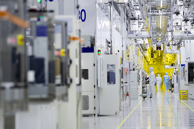
Samsung Foundry revealed its latest process technology roadmap today at its annual Samsung Foundry Forum (SFF) 2023. The company's SF2 (2 nm-class) production node is on track for 2025, whereas its successor SF1.4 (1.4 nm-class) is expected to be available in 2027. Meanwhile, the company published some of the characteristics it expects from its SF2 manufacturing process.
Samsung's SF2 process technology, which will be available to the company's clients in 2025, will offer a 25% higher power efficiency (at the same clocks and complexity), a 12% increase in performance (at the same power and complexity), and a 5% decrease in area when compared to SF3, the company's 2nm Generation 3 nm-class node introduced earlier this year. To make its SF2 technology more competitive, Samsung intends to offer the node with a portfolio of advanced IP for integration into chip designs, including LPDDR5x, HBM3P, PCIe Gen6, and 112G SerDes.
Samsung's SF2 will be followed by SF2P optimized for high-performance computing (HPC) in 2026, and then by SF2A, which will be aimed at automotive applications, in 2027. Around the same year the company intends to start mass production using its SF1.4 (1.4 nm-class) fabrication process.
Samsung's 2 nm-class node will be available around the same time as TSMC's N2 process technology (2 nm-class) and about a year or more after Intel's 20A process.
Samsung also plans to keep advancing its radio frequency technologies. The company expects its 5 nm RF process technology to be ready in in the first half of of 2025. When compared to the older 14 nm RF process, Samsung's 5 nm RF is projected to increase power efficiency by 40% and increase transistor density by around 50%.
Also in 2025, Samsung will initiate production of gallium nitride (GaN) power semiconductors for various applications, including consumer products, datacenters, and automotive sector.
In addition to expanding its technology offerings, Samsung Foundry remains committed to expanding its manufacturing capacities in Pyeongtaek, South Korea, and Taylor, Texas. Samsung intends to start mass production of chips at its Pyeongtaek line 3 (P3) in 2H 2023. Construction of the new fab in Taylor is expected to be completed by the end of the year, with operations commencing in the second half of 2024. The foundry's current plans is to increase its clean room capacity by 7.3 times by 2027, compared to the capacity in 2021.
Source: Samsung


4 Comments
View All Comments
ballsystemlord - Tuesday, June 27, 2023 - link
But their 5nm isn't even working right last I heard. How will they get to 2nm on time if they can't manage 5nm?ET - Wednesday, June 28, 2023 - link
Samsung's 4nm was recently reported to have yields similar to TSMC's.iphonebestgamephone - Wednesday, June 28, 2023 - link
What about efficiency?pogsnet - Friday, July 14, 2023 - link
Intel can't be ahead with Samsung in process technology, Intel can't even have 5nm, 4nm or 3nm now they are ahead with 2nm?Intel is full of talks no output in terms of foundry.