Amkor to Build $2 Billion Chip Packaging Fab in Arizona Primarily for Apple
by Anton Shilov on December 4, 2023 2:00 PM EST- Posted in
- Semiconductors
- Apple
- Packaging
- 3D Packaging
- Amkor

Amkor, the world's second largest independent outsourced semiconductor assembly and test (OSAT) service provider, has announced their intention to build a new advanced chip packaging facility in the U.S. Carrying a price tag of around 2 billion dollars, the plant in Arizona will primarily serve to package chips produced by TSMC at its Fab 21 nearby.
Adding an interesting (and unusual) wrinkle to the announcement, the notoriously tight-lipped Apple also issued its own press release, officially confirming that it is set to become the largest customer of the facility. All of which has greatly raised the profile of the chip packaging plant.
Huge Packaging Facility
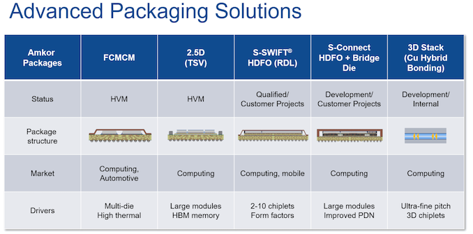
The planned facility will reside in a huge manufacturing campus covering 55 acres near Peoria, Arizona. Amkor does not disclose planned production capacity of the plant or technologies that it will support, but it says that it will serve automotive, high-performance computing, and mobile applications, so we can expect it to support a wide range of 2.5D and 3D packaging technologies.
Meanwhile, the company says that it its upcoming facility will feature 500,000 square feet (46,451 square meters) of cleanroom space when it is fully built and equipped. To some degree, the $2 billion investment implies that the plant will be quite vast. For example, TSMC's upcoming advanced manufacturing facility expected to come online in 2027 is set to cost $2.87 billion. The facility is expected to become operational in 2025 –2026 and employ some 2,000 people.
Amkor clearly aims that its Peoria facility will serve clients that produce chips at TSMC's Fab 21, which will greatly simplify their supply chain and will add value for those who need to develop, produce, and package chips in the United States. What is particularly important is that Amkor and Apple say they had worked in close partnership to design the strategic and manufacturing capacity aspects of the Peoria facility.
"Apple is committed to help build a new era of advanced manufacturing, right here in the US,” said Jeff Williams, Apple's chief operating officer in a statement. "Apple and Amkor have worked together for more than a decade packaging chips used extensively in all Apple products, and we are thrilled that this partnership will now deliver the largest OSAT advanced packaging facility in the United States."
This is where it gets interesting.
Tailored for Apple's Needs
This collaboration suggests that the factory will be specifically geared towards meeting Apple's requirements in the next few years. Apple will be the first and primary customer of this facility, utilizing it for packaging and testing chips from TSMC's nearby Fab 21.
"Apple silicon has unlocked new levels of performance for our users, enabling them to do things they could never do before, and we are thrilled that Apple silicon will soon be produced and packaged in Arizona," said Williams.
TSMC's Fab 21 phase 1 is now set to start making chips on 4 nm and 5 nm-class process technologies sometimes in 2025. Following this, the phase 2 of Fab 21 is expected to start producing chips on TSMC's 3 nm-class technologies sometimes in 2026. The timing of Amkor's facility becoming operational aligns with these developments, indicating that Apple will have a substantial need for packaging 3nm and 4nm-class chips around that time.
Typically, Apple is the first company to adopt TSMC's leading-edge technologies for use in high-volume products. For example, for this year's iPhone 15 Pro smartphones and MacBook Pro laptops, Apple uses TSMC's N3B fabrication process to make the A17 Pro, M3 Pro, and M3 Max SoCs. But at the same time Apple hasn't done a wholesale cutover to N3B; the company continues to use their N4-based A16 Pro and N5P-based M2 SoCs for its respective current-generation iPhone 15 and MacBook Air products. So Apple's total chip needs remain spread over multiple generations of nodes.
Ultimately, with TSMC's US fab set to remain a node behind its Taiwan fabs, the significant commitment from Apple to use Amkor's US packaging plant is a strong sign that the company will continue to make significant use of older nodes going forward.
CHIPS Funding
Finally, to ensure the advanced packaging project's success in the U.S., Amkor has applied for funding from the CHIPS program, which focuses on advanced chip packaging. The facility is a strong candidate for this government funding, as it will significantly strengthen the American semiconductor supply chain and enable TSMC’s Fab 21 customers in Arizona to access advanced packaging methods without having to transport their wafers out of state.
Source: Apple


12 Comments
View All Comments
Threska - Monday, December 4, 2023 - link
Hopefully not delayed like the TSMC plant for lack of qualified people.PeachNCream - Monday, December 4, 2023 - link
I've heard from various sources that its rather difficult to find highly skilled workers in the States and that it's been a problem for at least a decade. There are a fair number of reputable institutions, but an apparent shortfall nonetheless. Does anyone know the causes? Are people training other skills?lmcd - Monday, December 4, 2023 - link
The cause is that anything practical is deemed as "a trade skill" is simply an "application of the theory we teach" and surely can be learned by the student in their free time.HaninAT - Tuesday, December 5, 2023 - link
It seems to me, that the true issue is an inability to talk US workers into anything more than 8hr/5day work periods nor any of the other restrictions that US works, and really any laborer in any other country should, have come to expect. Breaks, sick/holiday time and the rest are probably off the table for TSMC. By Highly Skilled, they really mean, willing to do anything for little pay and long hours with no job security in sight.hbsource - Wednesday, December 6, 2023 - link
Wait until you discover what Europeans get then you'll understand why this plant is being built in the US.In the UK (which is far from the most generous) parents can share 50 weeks of parental leave between them when a child is born. Employers must hold their job for their return.
drwho9437 - Thursday, December 7, 2023 - link
They can certainly be talked into it but TSMC isn't used to having to pay a premium for that, and in the US and EU they will have to do it to get labor to work the night shift, because people can get other work if they are smart enough to do FAB work.As far as training. Honestly, I have been in FABs most of my adult life as a researcher, you can spend 1-2 months on someone hands on and make them useful. It isn't that complex. The engineering is but not the maintenance. Its going to be copy exactly anyway. The workers don't need to understand the statistics of EUV shot noise and defects to maintain the tools.
gdansk - Wednesday, December 6, 2023 - link
It's lack of experience in some areas. Constructing & operating fabrication facilities is a lost art in the US outside of Oregon.pugster - Tuesday, December 5, 2023 - link
They only announced it, no shovels in the ground yet. I will believe it when I see it.drwho9437 - Thursday, December 7, 2023 - link
I'd say this is basically not true, and an excuse. TSMC doesn't know how to operate in the US yet, that is a learning curve as well. Is Samsung saying they need to slow down? Micron? Intel? Ti? They are all building new FABs in the US right now. Only TSMC is saying this. The difference is all those others already play in the US.There will be a labor shortfall because so much capacity is coming online at similar times but if it was real now others would be slowing their roll outs more and honestly we don't see that (yet).
ballsystemlord - Friday, December 8, 2023 - link
I'd like to suggest that the other companies get people coming right out of college. Then they have the people sign non-compete agreements. Then no one can work at TSMC.