‘Better Yield on 5nm than 7nm’: TSMC Update on Defect Rates for N5
by Dr. Ian Cutress on August 25, 2020 9:30 AM EST
One of the key metrics on how well a semiconductor process is developing is looking at its quantitative chip yield – or rather, its defect density. A manufacturing process that has fewer defects per given unit area will produce more known good silicon than one that has more defects, and the goal of any foundry process is to minimize that defect rate over time. This will give the customers better throughput when making orders, and the foundry aims to balance that with the cost of improving the manufacturing process.
The measure used for defect density is the number of defects per square centimeter. Anything below 0.5/cm2 is usually a good metric, and we’ve seen TSMC pull some really interesting numbers, such as 0.09 defects per square centimetre on its N7 process node only three quarters after high volume manufacturing started, as was announced in November at the VLSI Symposium 2019. As it stands, the defect rate of a new process node is often compared to what the defect rate was for the previous node at the same time in development. As a result, we got this graph from TSMC’s Technology Symposium this week:
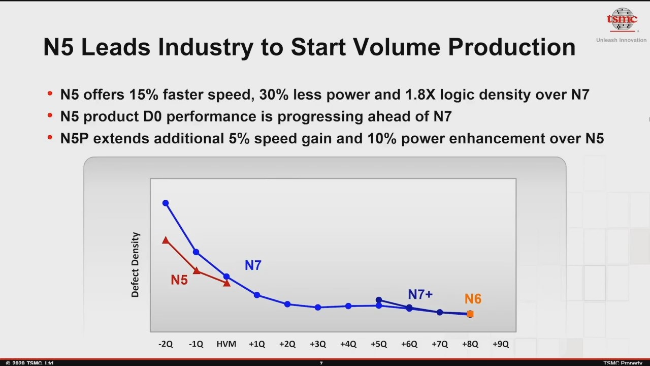
As it stands, the current N5 process from TSMC has a lower defect density than N7 did at the same time in its development cycle. TSMC. This slide from TSMC was showcased near the start of the event, and a more detailed graph was given later in the day:
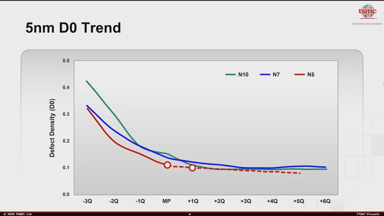
This plot is linear, rather than the logarithmic curve of the first plot. This means that TSMC’s N5 process currently sits around 0.10 to 0.11 defects per square centimeter, and the company expects to go below 0.10 as high volume manufacturing ramps into next quarter.
Part of what makes 5nm yield slightly better is perhaps down to the increasing use of Extreme UltraViolet (EUV) technology, which reduces the total number of manufacturing steps. Each step is a potential chance to decrease yield, so by replacing 4 steps of DUV for 1 step of EUV, it eliminates some of that defect rate.
TSMC’s first 5nm process, called N5, is currently in high volume production. The first products built on N5 are expected to be smartphone processors for handsets due later this year.
Related Reading
- TSMC Details 3nm Process Technology: Full Node Scaling for 2H22 Volume Production
- TSMC To Build 5nm Fab In Arizona, Set To Come Online In 2024
- TSMC & Broadcom Develop 1,700 mm2 CoWoS Interposer: 2X Larger Than Reticles
- TSMC Boosts CapEx by $1 Billion, Expects N5 Node to Be Major Success
- Early TSMC 5nm Test Chip Yields 80%, HVM Coming in H1 2020
- TSMC: 5nm on Track for Q2 2020 HVM, Will Ramp Faster Than 7nm
- TSMC: N7+ EUV Process Technology in High Volume, 6nm (N6) Coming Soon


102 Comments
View All Comments
FreckledTrout - Tuesday, August 25, 2020 - link
Looks like N5 is going to be a wonderful node for TSMC. Like you said Ian I'm sure removing quad patterning helped yields. Also switching to EUV the "lines" drawn are less fuzzy which will lead to better power and I have to assume higher frequencies at least higher frequencies on average. That last part is the killer for AMD right now as only 1-2 cores are able to hit rated frequencies and I'm pretty certain its due to quad patterning but do not know that for fact.psychobriggsy - Tuesday, August 25, 2020 - link
Marvell claim that TSMC N5 improves power by 40% at iso-performance even, from their work on multiple design ports from N7.https://semiaccurate.com/2020/08/25/marvell-talks-...
FreckledTrout - Tuesday, August 25, 2020 - link
Interesting read. The N5 node is going to do wonders for AMD.michael2k - Tuesday, August 25, 2020 - link
It'll be phenomenal for NVIDIA. They're currently at 12nm for RTX, where AMD is barely competitive at TSMC's 7nm. I've heard rumors that Ampere is going to 7nm, which is going to keep them ahead of AMD probably even at 5nm. I have no clue what NVIDIA is going to do with the extra die space at 5nm... other than more RTX cores I guess.Kamus - Tuesday, August 25, 2020 - link
All the rumors suggest that nVidia went with Samsung, not TSMC.The reason is, they tried to play hardball with TSMC, and wanted lower prices. They threatened to leave to Samsung if they didn't get their way.
Obviously, TSMC was smart enough to tell them to fuck right off, and by the time they realized Samsung's node was hot garbage compared to TSMC, it was too late... there was no capacity left.
Rumors also say, that they do have enough capacity in lockdown for 5nm...
So as big as an upgrade ampere is going to be (which would'be been at least 20% larger on TSMC) compared to Turing, it will be very short lived, since they can either to a 7nm refresh on TSMC, or better yet, a 5nm GPU sometime next year.
Things haven't been this interesting in at least a decade... 2020-2022 are going to be huge. Hopefully they can keep the momentum going for longer than that though.
whatthe123 - Tuesday, August 25, 2020 - link
The rumor is based on them having a contract with samsung in 2019. There's no rumor that TSMC has no capacity for nvidia's chips. A100 is already on 7nm from TSMC, so it's pretty much confirmed TSMC is working with nvidia on ampere. Only thing up in the air is whether some ampere chips from their gaming line will be produced by samsung instead.Kamus - Thursday, August 27, 2020 - link
"Only thing up in the air is whether some ampere chips from their gaming line will be produced by samsung instead."That's not what is being said...
That was their plan, but trying to play hardball with TSMC backfired, and the rumor is that they just wouldn't be able to make enough gaming chips on TSMC.
The early rumor was that the low end graphics cards would be on Samsung, and all of the high end chips would be on TSMC. But apparently, that didn't work out, and they're going to have to make everything on Samsung's significantly inferior node.
There's a reason the cooler on the 3090 is a mammoth (which would be a good idea for ALL cards IMO, since it would help with noise control) and it's not just to keep the card quiet...
The card will require 3, 8 pin connectors. The node is bad, so they'll have to put a lot of power in to get to the performance target they want.
So all of the TSMC capacity will go to the highest paying customers (A100 buyers) and the rest of us are going to get second hand stuff.
JlHADJOE - Wednesday, August 26, 2020 - link
Nvidia IS on TSMC, but they're obviously using all their allocation to produce A100s. They have at least six supercomputer projects contracted to use A100, and each of those will need thousands of chips.https://www.hpcwire.com/2020/08/19/microsoft-azure...
Obviously they'll prioritize their big expensive HPC chip with huge margins over the consumer stuff which is why RTX3000 gets booted to Samsung 8nm. I'd expect a 3000 Super built on TSMC a year from now after demand for A100 is filled and Nvidia can use their allocation for something else.
https://videocardz.com/newz/nvidia-a100-ampere-ben...
AnGe85 - Wednesday, August 26, 2020 - link
Currently, the manufacturer is nothing more than rumors. The only available facts are:- GA100 is manufactured on TSMCs N7
- NV also hat 8LPP capacity ordered and e. g. it is known, that the Orin SoC is going to be manufactured in 8LPP
- J.Huang stated in December, that most of the new GPUs will be manufactured at TSMC, Samsung will only handle the smaller part
Kamus - Thursday, August 27, 2020 - link
"-- J.Huang stated in December, that most of the new GPUs will be manufactured at TSMC, Samsung will only handle the smaller part"Yeah, that was the plan... but it din't work out for them, they got greedy, but probably won't get punished by consumers since it will still be a huge upgrade over the current linup.
I'm hoping that AMD does enough to punish them for us though, Big Navi should give the regular 3080 a run for it's money.